Enginursday: Innovative Testbed Design (Part 2 of 2)
Join us for part two of our in-depth look at testbed design at SparkFun. Here, we focus on the hardware design choices for our in-house testing tool, the Flying Jalapeno.
This is part two of our series about the history of quality control and testbed design at SparkFun (click here to read part one). There was actually much discussion in the comments about hardware design - thank you so much to all that chimed in! You had very valuable feedback, and I look forward to hearing more after we dive a little deeper into the hardware on this design.
You are welcome to download the Eagle design files from the project GitHub repository here:
For more info on getting started with Eagle, please check out this tutorial: How to Install and Setup Eagle.
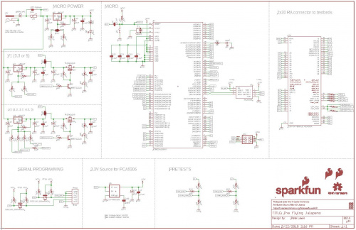
For anyone that might prefer to follow along with a PDF, you may also click on the following image:
Power control switching
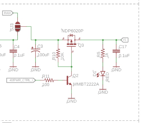
One of the earliest advancements in testbed design was the ability to control when power is applied to the product. Before this feature, we usually left the pogopin to the product’s VCC “HOT” - meaning that it was permanently wired to a power source. This should work fine, in theory, for most of the time, but what we found was that if you didn’t place the product down perfectly, sometimes you would momentarily short VCC to GND. Note, this would only happen on products where the two header pins VCC and GND were located next to each other, but that was actually pretty common. So during this burst of current on VCC, our testbed power supplied didn’t really like this, and they would drop voltage causing the entire testbed to reset. Ugh!
Some of the first testbeds to incorporate power control actually just routed an IO pin directly from the testbed ATMega328 to the VCC on the product. In this case, we could supply power to the product, but were limited to the 40mA (or so) that the IO could provide. Definitely not the best solution, and we saw a few testbeds die, and so the progress continued.
|
|
| Power switch schematic close up | Power Switch highlight on board |
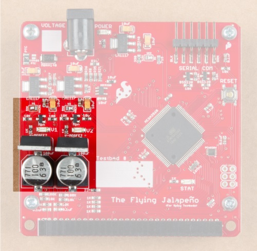
The next approach was to try a high-side switch using a mosfet. Looking back, we could have just as easily done it with a relay, but didn’t have an ideal relay in our inventory. Now that we have some nice mini relays like the SparkX Qwiic Relay, that may be the preferred way. But at the time (2009-ish), we only had the Beefcake Relay Control Kit, which seemed like overkill for 99 percent of our products. You’ll notice we also added a transistor on the front end to ensure the mosfet opens fully and takes the load off of the IO pin on the micro, and it’s really quite nice that writing the control pin HIGH actually engages power. We are always trying to think about usability, even with in-house tools.
Testing for shorts to ground
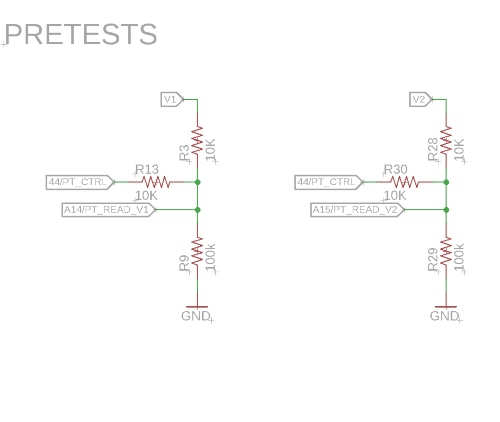
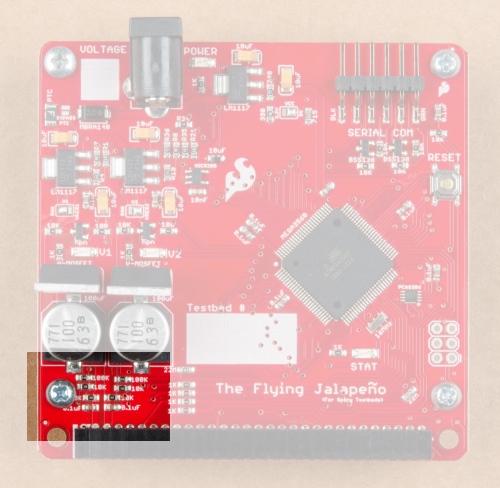
Using a simple voltage divider style circuit, a digital control pin and an analog read pin, we can safely and easily test a product's power line (aka VCC) for a short to GND. It is particularly nice to know this before powering up a product - especially when it is a high-current product. We actually test for shorts to GND on all products now, regardless of power consumption. Odds are the testbed and product would survive a few hundred surges, but after a few too many, you are on the quick path to destruction. When designing for production, we need to think about testbeds living on (and working well) for many years to come.
I should also note that we commonly refer to this test for shorts to GND as the “pre-test.” This is because the “main” test is usually referred to as just the “test.”
The pre-test circuit is actually a pretty good exercise in learning about voltage dividers. If you’d like to learn more check out this tutorial here.
|
|
| Pre-test for shorts to ground schematic close up | Pre-test highlight on board |
We use the circuit shown above to see whether or not there is a GND connection (or something that pulls as much current as GND would) on the product’s VCC. When there is a short, then the two 10K resistors basically split the VCC and the ADC reads the magic dreaded “486.” When there is no short, it will essentially form another voltage divider between a 100K and a 10K, and the ADC reading will be much higher. For a more info on this circuit, please check out a previous blog about quality control here.
Capacitive Touch "Buttons"
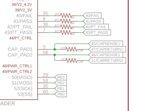
We moved away from mechanical momentary switches to engage testing years ago. A capsense pad (most importantly, non-mechanical) is much more reliable over thousands and thousands of “presses.”
|
|
| Capacitive Sense schematic close up | Capacitive Sense Resistors highlight on board |
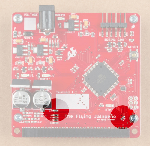
We use the Arduino capacitive touch library and two IO pins with a large resistor. Because we often need two buttons on a test fixture, we opted to dedicate four IO pins and include the resistors into the Flying Jalapeno design. With this setup, we simply need to route a trace to a pad on the daughter testbed. Note: we do usually take extra care on these traces and route them with 0.02 inch (20 mils) width. By avoiding vias and other data lines, we have seen great results with this form of capsense. Mad-house-routed thin traces or bad ground pour flow can make for some really wonky readings.
Dedicated LED IO with Built-in Resistors
We pretty much always need four LEDs on the testbeds these days – PASS/FAIL for the pre-test for shorts to GND, and PASS/FAIL for the main test. Because we have plenty of extra IOs on the ATMega2560, we decided to include the current limiting resistors on the FJ. These pins are now fairly committed for LED use, but we’ve got plenty of IOs to spare. This way, the daughter boards simply need a trace to an LED on each of these lines. The less complex the daughter boards can be, the better!
I2C Isolation “Switch”
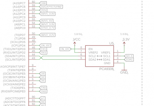
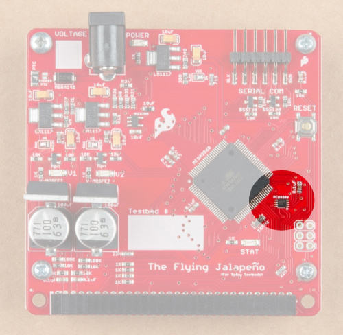
A lot of early testbeds that involved I2C were troublesome for us. It was pretty common for I2C testbeds to “lock up” during testing. This was usually due to the testbed trying to talk to a product that was broken, had cold solder joints or had jumpers on SDA or SCL. I seem to remember a glorious day when wire.end() actually started working... Until then, we used to (and still do) disconnect the lines with a mux built into the test fixture.
|
|
| I2C "isolation" switch schematic close up | I2C "isolation" switch highlight on board |
Again, at the time, we didn’t really have an ideal switch, and the Beefcake seemed like overkill for data lines, so we opted to use the PCA3906 I2C converter IC we had on hand. It had an enable pin that proved to be useful in disconnecting. We found that if we disconnected the I2C lines with something like this (in between testing boards), then it was much less likely to lock up. And best of all, the techs were much less likely to wear out the old fashioned momentary reset button the test fixture.
ATMega2560
|
|
| ATMega2560 schematic close up | ATMega2560 highlight on board |
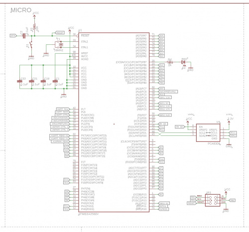
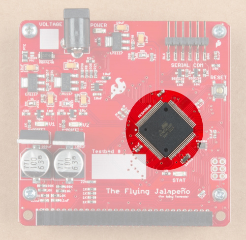
We simply went with this because it was very similar to our RedBoard, but with many more IOs. Sometimes a testbed will require a few more IO than the ATMega328 has to offer, so we found ourselves either using a mux or shift registers – better safe than sorry when it comes to having enough IOs. Also, having an Arduino-compatible testbed brain meant that we could more often than not utilize some of the product example codes for the test fixture.
The test developer also serves as a good beta tester for the products they work on. Usually the engineer on the product design has some sort of working code ready before we launch (which is super handy for test development). But sometimes even more importantly, getting it to work on the test fixture can help discover some bugs or documentation confusion before we officially go live with it on SparkFun.com.
Logic Level Select Jumper
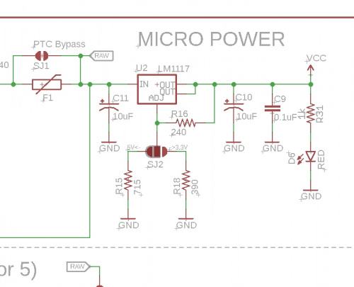
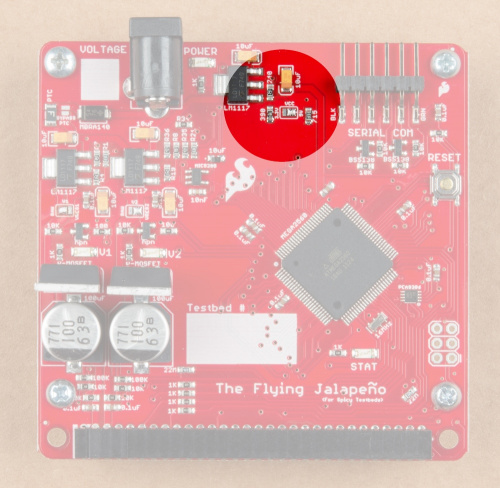
Taking a tip from our breadboard power supply, we opted to add in a logic level select jumper.
|
|
| Logic Level Select schematic close up | Logic Level Select highlight on board |
There was some discussion as to whether we wanted a slide switch or jumper. We ultimately wanted to keep it a jumper, so that it couldn’t be accidentally switched during handling and cause issues for testing. Plus, there is always gonna be some soldering assembly work for the daughter boards, so what’s the trouble in setting a quick jumper as well? Also, you may note that we are doing a “no-no” here by running the ATMega2560 at 3.3V - it is slightly out of spec for a 16MHz crystal, but we have seen minimal issues (if any at all) caused by this, so we’re gonna keep running with it.
Software-Definable VReg Control on Two Power Sources
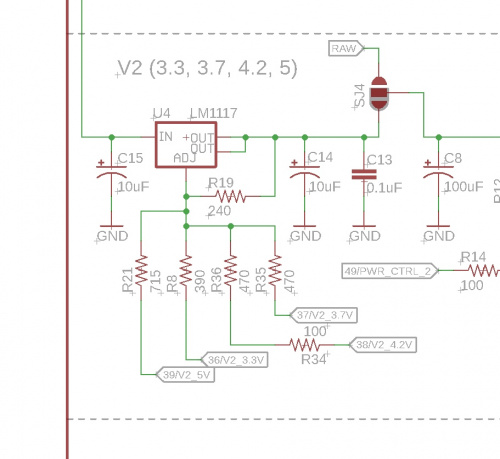
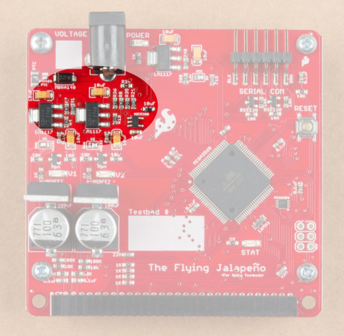
Taking the selectable VReg idea one step further, we decided to make the two power sources have adjustable outputs that were software defined. By connecting various resistors to IO on the micro, we can choose which resistor we’d like to “send to GND” by writing that corresponding IO LOW. This effectively sets the output of our VRegs.
|
|
| Software Definable Voltage schematic close up | Software Definable Voltage highlight on board |
You'll notice that V1 can do 3.3V or 5V, and V2 can do 3.3, 3.7, 4.2 or 5V. This is nice when emulating a charged or empty single cell LiPo battery. By bouncing V2 between 3.7 and 4.2, we can get charge circuits to engage or disengage. This has proven very handy when it comes to getting a charge LED to blink.
2x30 RA Header
There was much discussion about what type of connector would do the job. It was tough to find the balance between strength, current capabilities, size and design-ability. We opted to go with a PCB-to-PCB right-angled style connector, and the 2mm pitched RA 2x30 header we found had a 2A rating, so it fit the bill. We also opted to have some connections with redundant pins (GND, V1, V2). Not only was this a good thing for reliability, it gave us way more current capability than we’d ever need (famous last words). More connection means less resistance too, so I was glad to know we’d see very minimal voltage drop from source to pogopin.
Mounting Brackets
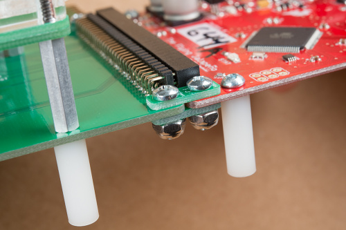
With our choice of connector, this required a little creativity on how to mechanically connect the FJ to the daughter boards. We did not want to rely solely on the headers themselves, and so came up with some mounting brackets on either side.
They go on either side of the connector, on the top and the bottom, and are held into place with a 4-40 screw with a nylon thread locking nut. The spacing of the drill bits also ensures that the FJ and the daughter board will be assembled at the exact spacing for every future testbed. This is nice, because we want to make sure that the 2x30 is inserted fully. Yet another benefit that I didn’t anticipate (and was pleasantly surprised while building up the first prototype), is that these brackets worked as a nice “jig” to hold them together while soldering in the 2x30 male connector on the daughter board.
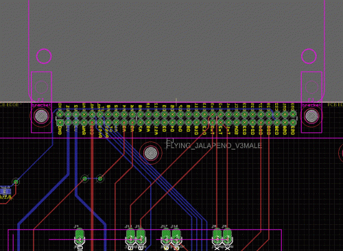
Custom Eagle Part
|
|
| Eagle Symbol | Eagle Package |
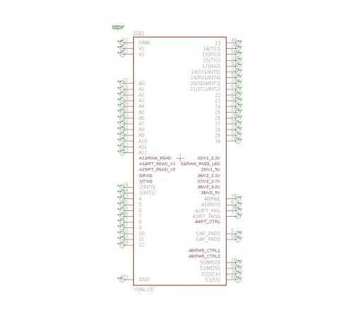
To make daughter board design faster, we opted to create a custom part in Eagle. This way, we could quickly drop in an FJ into any daughter board design, and have all of the connections easily accessible. Note: we created the female and male versions of the connector in the same device. This makes it easier when referencing the FJ design during any troubleshooting. Also, we opted to include quite a bit of “used pins” in the symbol, which help highlight what they are doing upstream and can help with developing code for this hardware. Although, using the code library in conjunction with this hardware makes life even easier.
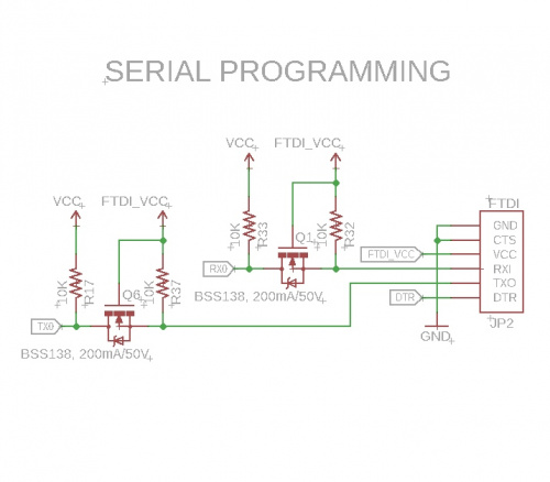
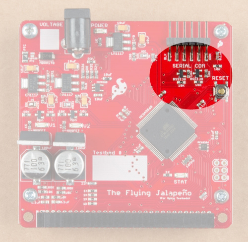
Logic Level Conversion for Serial Debug
|
|
| Serial Logic Level Conversion schematic close up | Serial Logic Level Conversion highlight on board |
Do you suffer from serial bridge logic level conversion problems? We do too. Around production and at most engineers' desks here at SparkFun, it is always impossible to find the right logic level version of the serial bridge. Also, it is probably one of the most common mistakes made around here - “whoops, I plugged in a 3.3V logic thing into a 5V thing,” or vice versa. Well, with the FJ, we had a chance to avoid this problem, so we did. A tech can plug in any variety of serial bridge tools into the FJ, and it has the logic level conversion to handle it. Whew!
A Future Hardware Revision
As with all projects, this will never truly be done. The Flying Jalapeno has some quirks that could be improved (thank you for all your feedback on our previous post). But after two rounds of prototypes, we are fortunate that nothing supercritical is a road blocker right now, and for the most part the Flying Jalapeno is doing its job quite well. Nevertheless, here are some of the things we are considering on the next revision:
Upgrade mux switch for I2C isolation. The original IC choice for the I2C isolation was not really the best IC for the job. When we need to switch a connection on most newer testbed designs, we opt to use the 74LVC4066 MUX 1:1 (x4). This has worked great for switching all of our RX/TX, USB D+/D-, and programming lines. We also used this on a recent programming tool for production: the Pi AVR Programmer HAT (https://www.sparkfun.com/products/14747), and it has been holding up well for all our 2MHz + programming speeds.
Additional GND connections on the right side of the header package. Sometimes it can be a challenge to get a good ground flow all the way around the daughter board, so if I were to do this again, I’d sacrifice a couple IOs to be GND connection points on the right side of the connecter.
Additional dedicated LED IO with resistors built in. We are finding that with most daughter boards, we usually need one or two more LEDs. In addition to the standard pass or fail LEDs, it’s nice to indicate the tech other statuses or instruct them that it is time to do a certain action. You can’t have too many LEDs!
A strange issue with power control. Maybe someone reading can help us with this, but strangely enough, the power control circuits seem to be interacting. When V1 is powered up, and V2 is powered down, there still is some voltage present on V2. We even tried removing the source of power on V2, and it shows the same condition. I’m guessing it has something to do with the two long traces perfectly parallel to each other. Most of the time, this is not a problem (because we have them both powered up during testing), so we've been able to get by with the current version of the hardware. But it sure would be great to get to the root of what's causing this, so any thoughts would be very welcome. Thanks!
Note, if you like to jump to part 1 of this blog, click here:
